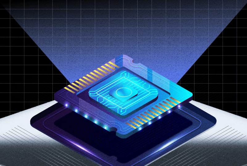
A new technology, 3D DRAM with integrated AI processing, has the potential to replace current High Bandwidth Memory (HBM). This innovation combines DRAM with AI capabilities, potentially leading to more efficient and powerful memory solutions, which could surpass existing HBM technology.
NEO Semiconductor, a company specializing in 3D DRAM and 3D NAND memory, has introduced its new 3D X-AI chip technology, which might eventually replace the current HBM used in AI GPU accelerators.
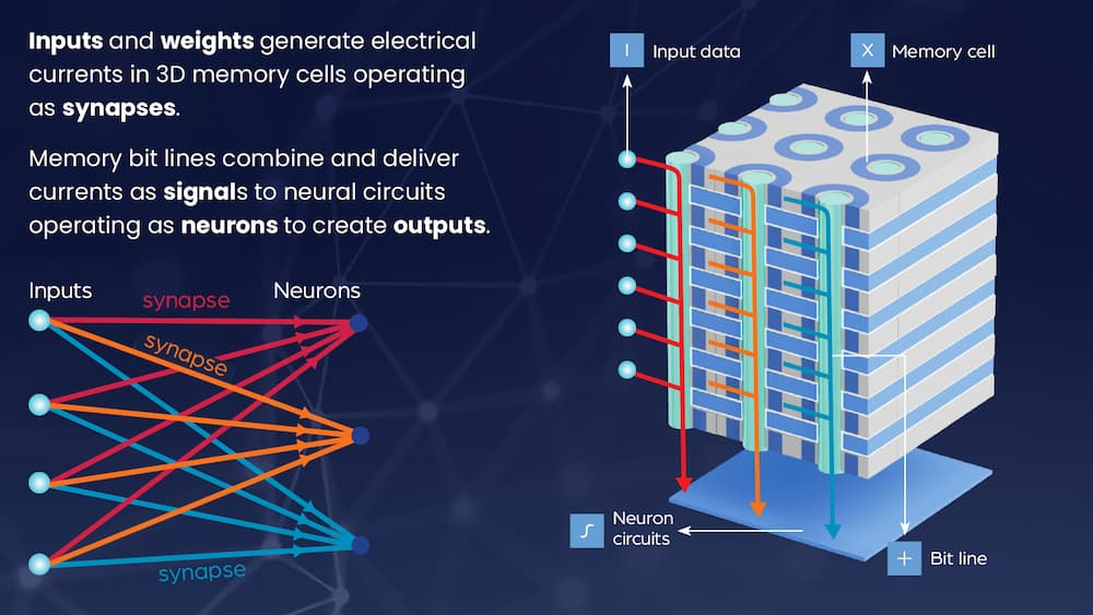
This 3D DRAM is said to feature built-in AI processing capabilities, allowing it to process and generate data without relying on mathematical outputs. By minimizing the data transfer between memory and processors, it can help alleviate data bus issues, boost AI performance, and lower power consumption.
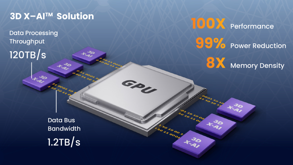
The 3D X-AI chip features an underlying neuron circuit layer capable of processing data stored across 300 memory layers within the same chip. According to NEO Semiconductor, with 8,000 neuron circuits handling AI processing directly in memory, the chip’s performance can be boosted by 100 times, and its memory density is 8 times greater than current HBM. Additionally, by decreasing the data processed by the GPU, power consumption can be cut by 99%.
A single 3D X-AI die includes 300 layers of 3D DRAM cells and a layer of neural circuits with 8,000 neurons. It has a capacity of 128GB and can support up to 10 TB/s of AI processing power. When 12 of these dies are stacked with HBM packaging, the processing throughput can reach 120 TB/s. NEO Semiconductor estimates that this setup could lead to a 100-fold increase in performance.
Andy Hsu, Founder & CEO of NEO Semiconductor, highlighted that current AI chips suffer from significant performance and power inefficiencies due to flaws in their architecture and technology. He pointed out that the current AI chip design stores data in HBM and depends on a GPU for all calculations.
Hsu also noted that separating data storage from processing has created a data bus bottleneck, limiting performance and leading to high power consumption during large data transfers.
According to Hsu, the 3D X-AI can handle AI processing directly within each HBM chip, which could greatly reduce the data transfer between HBM and the GPU, leading to significant improvements in performance and lower power consumption.
Many companies are exploring ways to boost processing speed and communication throughput. As semiconductor speeds and efficiencies improve, the data bus that transfers information between components could become a bottleneck. These new technologies aim to ensure that all components can accelerate together.
According to a report from Tom’s Hardware, companies such as TSMC, Intel, and Innolux are investigating optical technologies to enhance communication speeds within motherboards. NEO Semiconductor’s approach of shifting some AI processing from the GPU to HBM could reduce the GPU’s workload, potentially achieving greater efficiency than current power-intensive AI accelerators.